
 k-Space Associates, Inc. is proud to announce that the kSA Emissometer ex situ metrology tool for MOCVD carrier characterization now has ultraviolet (UV) photoluminescence (PL) capabilities for even better carrier evaluation.
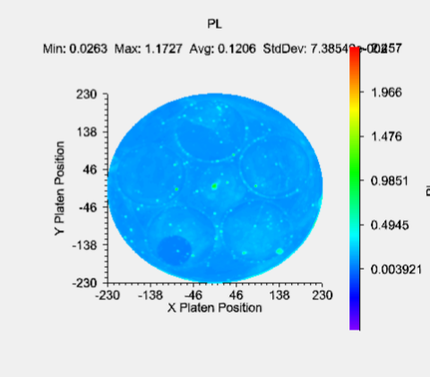
The new UV PL feature allows wafer carrier manufacturers, reactor manufacturers, and epi houses to further evaluate their wafer carriers before use and throughout their lifecycle. This system uses a 365 nm LED focused on the wafer carrier and a filtered photodetector focused on the excitation point. The filter cuts off light for wavelengths shorter than 409 nm. This results in the ability to evaluate contamination on the wafer carrier.
The kSA Emissometer is used to determine the quality of the carrier bake after the deposition run, quantitative determination of real surface emissivity for temperature set-point adjustments, and microcrack detection. The kSA Emissometer also provides statistical analysis of each individual pocket and web for carrier quality evaluation.
Darryl Barlett, k-Space CEO, states, “This tool gives carrier manufacturers, reactor manufacturers, and epi houses a competitive edge because it allows them to quantify their carrier quality, ultimately leading to increased device uniformity and increased yield.”
For additional information on the UV photoluminescence feature and the product specifications, please visit https://k-space.com/products/ksa-emissometer/.
About k-Space Associates, Inc.
k-Space Associates, Inc. (www.k-space.com) is a leading metrology supplier of in-line, in situ, and ex situ metrology tools for the semiconductor, thin-film, photovoltaic (PV), solar, automotive, glass, and building materials industries. Founded in 1992, its systems are used to monitor dimensions, wafer temperature, thin-film stress, deposition rate, thickness, material absorption properties, and Reflection High Energy Electron Diffraction (RHEED). Backed by a commitment to ongoing support, these solutions are currently used worldwide in research and production line monitoring in multiple industries. Extensive input and close collaboration with its worldwide customer base have led to the development of today’s most powerful metrology tools.
