Monitor and control your sputtering deposition process with in situ metrology tools that optimize your thin-film quality. The right tools can give you the insight you need for sputtering results that stick!
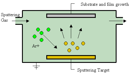 Sputter deposition is a PVD method of depositing thin films by plasma sputtering. Sputtering effectively “knocks off” the material to be sputtered via a high energy, ionized atom (typically Ar). The material sputtered or knocked off from the sputter target then impinges on and typically sticks to the substrate, usually a wafer. Sputtered atoms ejected from the target have a wide energy distribution, typically up to tens of eV.
The availability of many parameters that control sputter deposition make it a complex process, but also allow for a large degree of control over the growth and microstructure of the film. Being able to monitor and control the deposition process through the use of kSA in situ metrology tools provides great insight into these sputtering conditions.
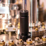
RHEED (Reflective High Energy Electron Diffraction) hardware from Staib and R-DEC can be used under higher pressure sputtering conditions that allow for shorter electron beam paths to avoid gas collisions. Being able to analyze the surface structure and morphology via electron diffraction on a phosphor RHEED screen via the kSA 400 RHEED system provides real-time film growth information. Growth rate, surface structure and texture, and lattice spacing/strain are easily determined using the kSA 400 RHEED system.
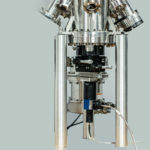
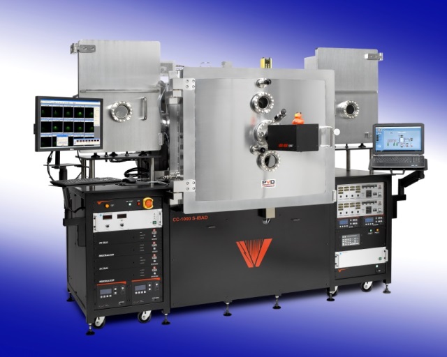
Standard sputtering systems currently being offered from PVD Products and AJA International provide these valuable in situ monitoring tools from k-Space as a standard option and are integrated into the deposition control software.
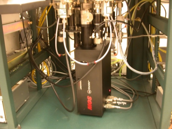
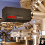
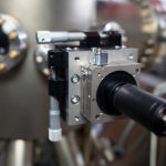
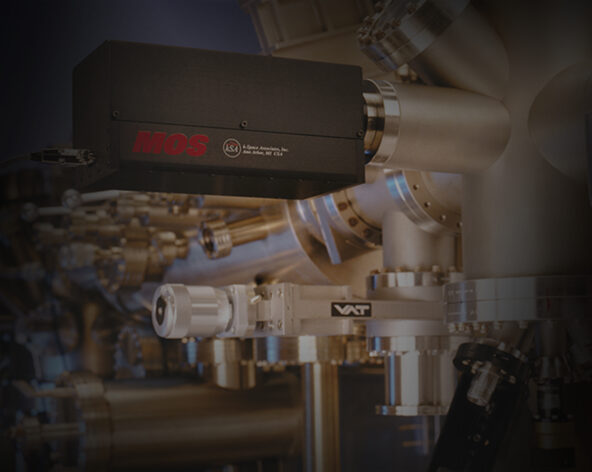
Stress measurement and control can give you key insights into your process and quality. Being able to measure the stress/strain in situ with the kSA MOS during the process gives important insight into mechanisms and methods for controlling and targeting the overall stress induced into the sample during every step.