Increase performance and quality with compact in situ tools for MOCVD. Discover the power of feedback control of wafer carrier/pocket temperature, film thickness, thin-film stress/wafer bow, and surface measurement in real-time.
- Overview
- Film Thickness and Growth Rate
- Temperature
- Curvature and Stress
- Wafer Carrier Characterization
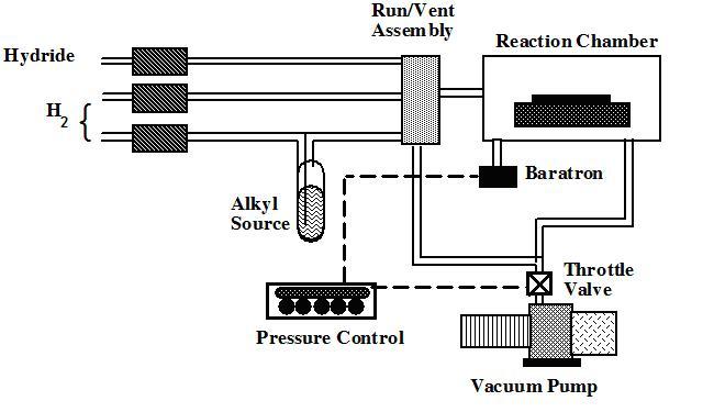
Metalorganic Chemical Vapor Deposition (MOCVD), sometimes called Metalorganic Vapor Phase Epitaxy (MOVPE), is a much higher throughput technique compared with MBE, and as such is the production deposition tool of choice for most compound semiconductor devices such as High Brightness LED’s (HBLED). Worldwide, there are several research-level MOCVD tool manufacturers, including Structured Materials, Taiyo Nippon-Sanso, Valence Process Equipment, Samco and others. However, at the production level, there are two companies that dominate sales and have over 90 percent of the collective market share: Veeco Turbodisc and Aixtron.
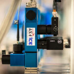
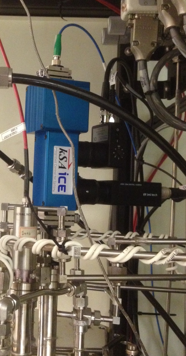
MOCVD relies on the gas phase transfer of the materials to be deposited on the substrate. The deposition ultimately occurs via a chemical reaction at the substrate surface and typically results in high quality, epitaxial thin-film deposition. Because MOCVD utilizes heated gas flow and surface chemical reaction, substrate temperatures for typical device growth are higher than MBE and in the 500-1500 degrees Celcius range. In addition, the sample can be rotated at speeds as high as 1500 RPM to promote higher uniformity and film quality. Furthermore, optical access is typically limited to less than 10mm, and the optical path distance is typically short (e.g. 250mm or less). In addition, MOCVD deposition occurs at pressures close to atmospheric pressure, which precludes in situ metrology that utilize electron beams or x-rays. For these reasons, in situ optical metrology probes for MOCVD are typically compact in size. The kSA ICE metrology tool is small, compact, and easy to use. This tool offers in situ direct substrate temperature, wafer carrier temperature, film thickness, thin-film stress/wafer curvature, and surface roughness measurement in real-time.
Film thickness, reflectance and growth rate can all be measured in real-time for process control. Using the kSA ICE reflectivity module, you can have the measurements you need for improved process control, quality and efficiency. Each layer can be triggered via an external trigger signal, or can be time-based.
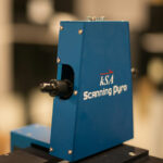
 Temperature plays a key role in the MOCVD process. Controlling it in real-time will provide you with the improved quality and efficiency you need. Temperature can be measured with both the kSA ICE emissivity corrected pyrometry temperature module and the band edge module. kSA ScanningPyro creates high resolution full temperature maps of Veeco K465i and EPIK700 wafer carriers and wafers. These maps are greatly enhancing the ability to perform process optimization.
 Real-time substrate curvature and film stress measured with the kSA ICE curvature module helps you monitor the stress induced during every step of the growth process and gives important insight into its dynamic behavior. This information enables you to better control both the wanted and unwanted stress in thin film to achieve the desired optoelectronic and mechanical properties.
 Quickly and easily generate high-resolution diffuse and specular reflectance and total emissivity maps of MOCVD carriers with the kSA Emissometer. Carrier emissivity variation means temperature non-uniformity, which can lead to reduced device yield and possibly complete growth run failure. Track emissivity changes to determine carrier end-of-life, without wasting growth runs. Detect unwanted residual deposits after baking, and easily identifies carrier surface defects, scratches, microcracks and pits that are not visible to the eye.