Obtain unmatched process efficiency and quality with powerful tools for RHEED analysis, and stress and temperature measurement and control.
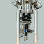
Molecular Beam Epitaxy (MBE) is an ultra-high vacuum (UHV) thin-film deposition technique. MBE is widely considered the most controllable and highest purity form of deposition and is currently used in both R&D and high volume production. Most MBE growth results in high-quality, epitaxial thin films.
Solid sources of high purity (5 nine or better) growth material are placed in crucibles, typically made of pyrolitic boron nitride (PBN). These crucibles are heated to the required evaporation temperatures for the given material, resulting in directed vapor flow of the evaporated material towards the substrate to be deposited on. Mechanical or pneumatically-based shutters are placed just above the crucibles, allowing for abrupt and accurate start/stop control of the deposition process.
Because of the purity of the source materials and the ultra-high vacuum environment (typically base pressures in MBE are 1 x 10⁻¹⁰ mbar or less), the deposited material is of the highest purity. Combined with accurate control of the substrate temperature, true atomic layer-by-layer deposition can be achieved, along with atomically abrupt interfaces between layers.
Using the right tools to measure and control this process is crucial for quality and efficiency.
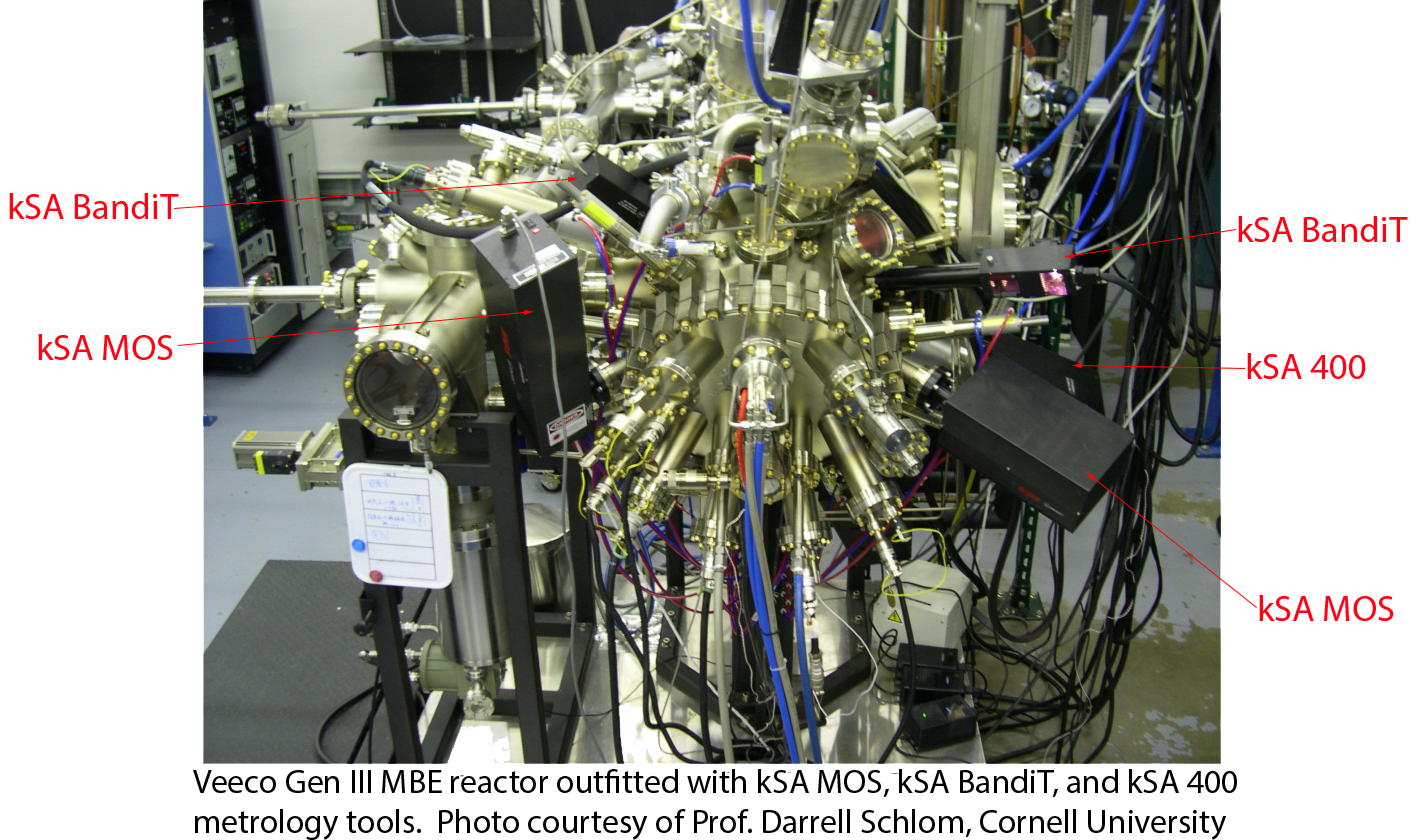
While there are a number of vacuum companies that make custom MBE systems, there are only a handful of commercial MBE reactor manufacturers worldwide. k-Space works with Veeco, Riber, DCA, SVT, Omicron, Eiko, and Anelva to ensure proper fitment and even advanced I/O communications into the growth control software. k-Space tools can be found worldwide on all these reactors.
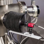
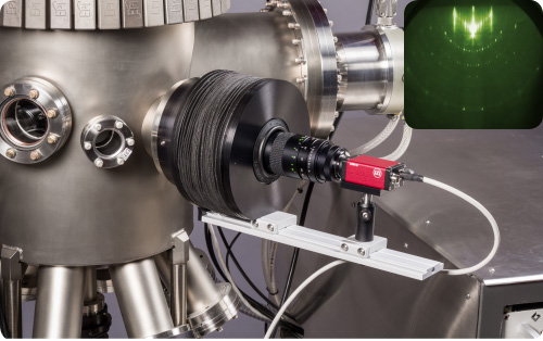
The most common in situ metrology tool used with MBE is Reflection High-Energy Electron Diffraction (RHEED). The RHEED technique utilizes a high energy (typically >= 15 keV) electron beam at grazing incidence to the substrate (typically 2°) to diffract off the surface layers and form a diffraction pattern on a phosphor screen. Analyzing the diffraction pattern can yield a wealth of information about the surface, including crystal structure, atomic spacing, surface quality, and growth rate. The kSA 400 Analytical RHEED system is designed to put all these surface features at your fingertips, and in real-time; it’s your window into the MBE growth process. See MBE at work with kSA 400.
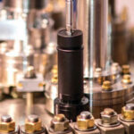
Substrate temperature is the most crucial growth control parameter for MBE (as it is for most deposition processes). However, it’s not easy to accurately measure the substrate temperature, as direct contact temperature measurement is not viable in MBE. Hence, most temperature control is done via monitoring the thermocouple embedded in the substrate heater element, but is not in direct contact with the sample. But a non-contact thermocouple is not representative of the substrate temperature, due to heat transfer losses, variation in substrate contact points, absorption/transparency of the substrate, and so on. IR pyrometers are commonly used for non-contact substrate temperature measurement. However, pyrometers are very susceptible to viewport coating and stray light (prevalent issues in MBE chambers), resulting in large errors in absolute temperature measurement.
k-Space has two options for your temperature measurement needs.
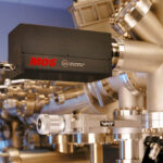
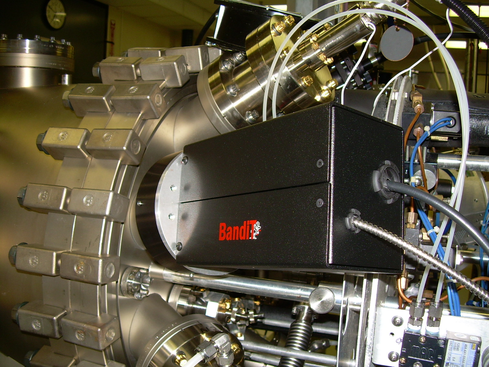
kSA BandiT temperature measurement system is immune to these problems, and has become the new standard for absolute and repeatable substrate temperature measurement in MBE.
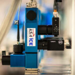
kSA ICE has an emissivity corrected pyrometry (ECP) module that can perform continuous temperature measurements at distances of up to 1m. kSA ICE with ECP is the preferred measurement tool for film deposition on small bandgap substrates (e.g. GaSb, InAs, Ge).
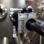
Because dissimilar materials are often deposited in MBE (e.g. InGaAs films on GaAs substrates or GaN films on Sapphire substrates), thin-film stress is an important parameter to monitor and ultimately control. Thin-film stress, which is attributable mainly to lattice mismatch and thermal expansion mismatch, can result in poor film quality and target device performance. In addition, too much thin-film stress yields large wafer bow, which can cause problems during lithography and device processing. The kSA MOS system accurately measures thin-film stress, curvature, and wafer bow using a patented multi-beam laser system. The kSA MOS system can be oriented in either a normal incidence (single port) or specular (two port) geometry on MBE reactors.