
In situ metrology manufacturer k-Space Associates, Inc. has installed a kSA BandiT non-contact optical temperature monitoring system on an Angstrom Engineering Quantum Series Josephson junction fabrication platform designed for a large commercial partner.
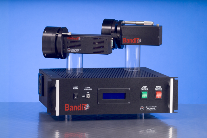 The kSA BandiT system is utilized in the oxidation chamber to monitor the substrate temperature in the room temperature to 250° C range. The non-contact measurement of temperatures in this regime is unique to k-Space by virtue of their patented band-edge-based temperature measurement technology.
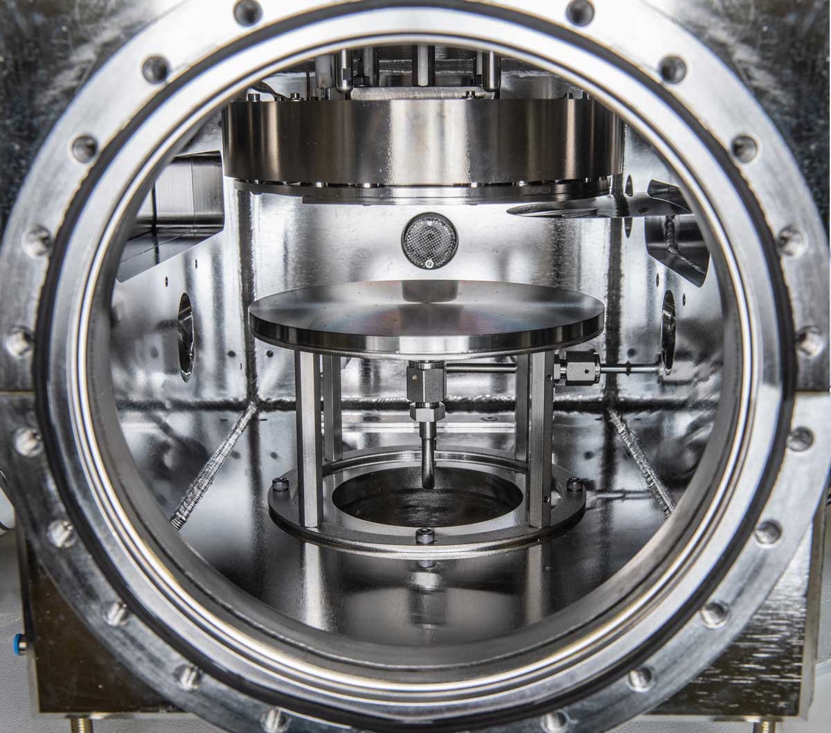
The kSA BandiT system was engineered to accommodate the fabrication system’s specific geometry and process materials. The oxide layer grown in this chamber is critical to the performance of the device and is largely influenced by the growth temperature. The ability to accurately measure the temperature of the wafer during oxidation creates a powerful level of control and should lead to a deeper understanding of this relationship.
Barry Wissman, a k-Space product development engineer and one of the kSA BandiT technology inventors said, “I am very impressed with Angstrom Engineering’s technology, and have enjoyed working with them on this project. Our BandiT instrument is able to accurately measure their substrate temperature in real time, even at low temperatures and in the presence of radiation from a substrate heating system. At k-Space we pride ourselves in the ability to customize our systems to provide the measurement and control capabilities our customers need to stay on top of their markets.”
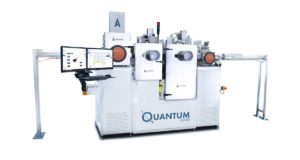
Angstrom Engineering’s Quantum Series equipment fabricates qubits for use in the exciting field of quantum computing. The Quantum Series Josephson junction fabrication platform utilizes physical vapor deposition, ion processing, gas flow management, precise substrate fixturing, and a pure vacuum environment to finely tune every variable of Josephson junction fabrication to the users’ requirements.
 “It has been a pleasure working alongside k-Space to bring this exciting low-temperature measurement technology to the quantum circuit fabrication community. The BandiT equips our Quantum Series of equipment with a powerful tool for direct, non-contact measurement of wafer temperatures during critical processes. We believe that this will provide researchers with a critical piece of information that can be used to optimize the quality and yield of quantum devices. Partnering with k-Space has allowed us access to world-leading technology and the knowledge and support of their helpful and talented staff – we are very happy to be working together,” stated Mike Miller, Director of Business Development at Angstrom Engineering.
To learn more about Angstrom Engineering’s Quantum Series capabilities for Josephson junction fabrication visit https://angstromengineering.com/products/quantum-series/. To learn more about k-Space non-contact low-temperature measurement visit https://k-space.com/products/bandit/.
About Angstrom Engineering
Angstrom Engineering Inc. specializes in the design and manufacture of high-quality physical vapor deposition (PVD) and chemical vapor deposition (CVD) equipment. Our partners are world-class academic, government, and commercial labs at the forefront of thin film research and applications, including quantum computing, superconducting circuits, renewable energy, thin film batteries, organic display and lighting, optics, semiconductors, and biosensors. Angstrom Engineering’s products range from small footprint PVD tools to fully automated, multi-chamber cluster tools.
We would be happy to have a conversation. Please contact us at:
Mike Miller, PhD
Director of Business Development
mmiller@angstromengineering.com
About k-Space Associates, Inc.
k-Space Associates, Inc. (www.k-space.com) is a leading supplier of advanced metrology instrumentation for the surface science and thin-film technology communities. Founded in 1992, its products are used for monitoring temperature, film stress, film thickness/deposition rate, as well as surface morphology. Backed by a commitment to ongoing support, these solutions are currently in use for both research and manufacturing of semiconductor-based electronic, optoelectronic, and photovoltaic devices. Close collaboration with its worldwide customer base has led to the development of today’s most powerful thin-film characterization products.
