
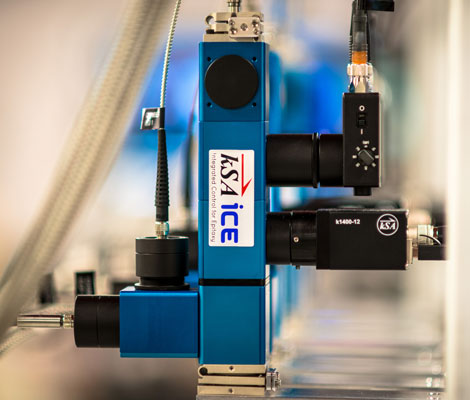
 Dexter, MI. July 27, 2015 – Sandia National Laboratories recently installed a kSA ICE tool on a modified EMCORE D-125 MOCVD reactor. The kSA Integrated Control for Epitaxy (kSA ICE) tool is a modular in situ metrology system capable of measuring multi-wafer real-time temperature, reflectivity, growth rate, film stress and substrate curvature during MOCVD processes.
This kSA ICE tool features the kSA patented reflectivity based pattern recognition software to keep track of individual wafers on this multi-wafer MOCVD system that does not have a locked carrier. It also features reflectivity at a wavelength of 405 nm, in addition to reflectivity at longer wavelengths of 660 and 960 nm. The 405 nm reflectivity capability will allow Sandia to better study defect formation and surface roughness with the goals of minimizing such defects and improving epitaxy processes and device performance.
Figure 1 shows the simultaneous measurement of 405, 660, and 960 nm reflectance during GaN template deposition on sapphire measured at Sandia. The 405 nm reflectivity does not produce interference oscillations as only the first surface reflection is measured – the light that penetrates the GaN is absorbed because it is above the band gap of the material. This technology can be used during well/barrier depositions to reveal differences in surface and interface quality that cannot be seen with longer wavelength light. Run-to-run comparisons of 405 nm reflectivity during well/barrier growth can potentially help improve device yield and reproducibility.
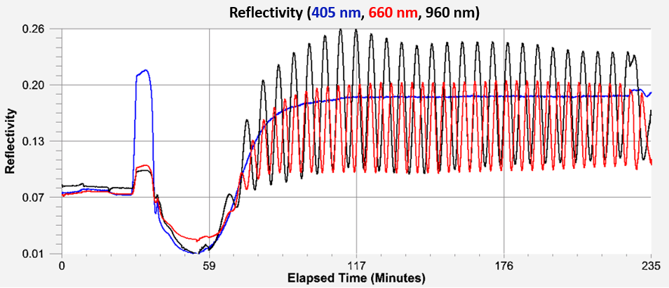
Figure 1: GaN reflectivity vs. time for GaN growth on sapphire at 405 nm, 660 nm and 960 nm as measured by kSA ICE on a modified Veeco D-125 reactor. Data courtesy of Dan Koleske at Sandia National Laboratories.
About k-Space Associates, Inc.
k-Space Associates, Inc. (www.k-space.com/) is a leading supplier of advanced instrumentation and software for the surface science and thin-film technology industries. Founded in 1992, its systems are used for monitoring wafer temperature, thin-film stress, deposition rate, thickness, material absorption properties, and Reflection High Energy Electron Diffraction (RHEED). Backed by a commitment to ongoing support, these solutions are currently used worldwide in research and production line monitoring of compound semiconductor-based electronic, optoelectronic, and photovoltaic devices. Extensive input and close collaboration with its worldwide customer base has led to the development of today’s most powerful thin film characterization products.
