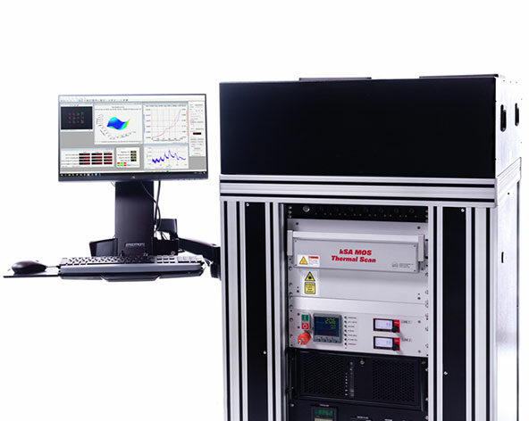
The kSA MOS UltraScan and kSA MOS ThermalScan systems are ex situ, flexible, high-resolution scanning wafer curvature, bow, and tilt-measurement systems.

The kSA MOS UltraScan and kSA MOS ThermalScan systems are flexible, high-resolution scanning wafer curvature, bow, and tilt-measurement systems. Based on proven and patented kSA MOS technology, the kSA MOS UltraScan uses a laser array to map the two-dimensional curvature, wafer bow, and stress of semiconductor wafers, optical mirrors, glass, lenses – practically any polished surface. For room temperature measurements, explore the kSA MOS UltraScan. If you want to know how your wafer changes with temperature, explore the kSA MOS ThermalScan.
For more information see the kSA MOS UltraScan Product Specification Sheet →
For more information see the kSA MOS ThermalScan Product Specification Sheet →
 Click to Enlarge
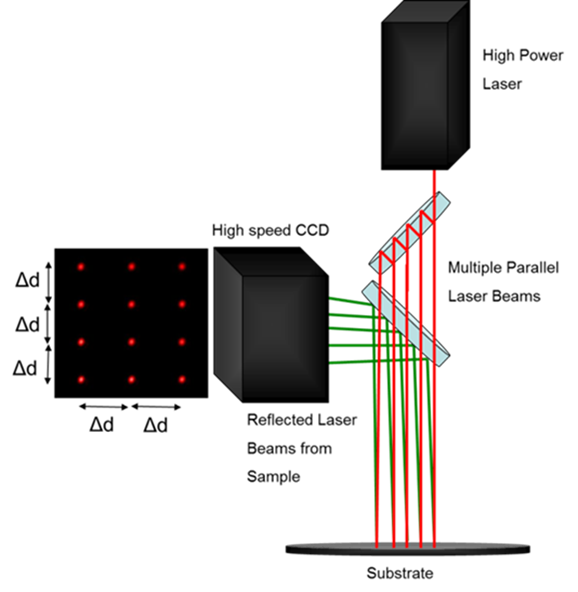
Laser Array Technique
The kSA Multi-beam Optical Sensor, or kSA MOS, technology is based on a patented approach which uses a single laser to generate a two-dimensional laser array. This laser spot array is then reflected off the sample surface into a high-resolution camera. Changes in the reflected laser array spot spacing at each point on the sample are used to determine the localized wafer curvature in both the X and Y direction. In this way, the system directly measures the curvature and stress in two dimensions simultaneously. This is something that single or dual beam curvature and stress tools simply
cannot capture.
 Click to Enlarge
Simultaneous Array Detection
Simultaneous detection of the laser array also makes the measurement inherently less sensitive to sample vibration compared with systems that rely on scanning the laser spot on the surface of the sample to measure the local curvature. This leads to kSA MOS’s increased wafer curvature resolution capability. Since all the laser spots move together at the same frequency, movement or tilt is not incorrectly detected as a change in sample curvature. Through the use of sophisticated image processing and data analysis algorithms, the kSA MOS UltraScan can easily detect micron-sized changes in spot position due to curvature changes, which translates to the highest wafer curvature/stress resolution metrology tool available.
The standard kSA MOS UltraScan system provides a 300 mm x,y scanning range for wafers or other reflective samples with better than 1 um scanning resolution. Optionally, larger scanning stages (larger glass panel mapping platforms) are available. Scans are fully programmable and extremely repeatable for selected area, line scan, or full area map of wafers. The system also provides quantitative film stress analysis with full area spatial map by first scanning the bare wafer and then re-scanning the wafer post-process. Unmatched curvature, stress, and bow analysis capabilities are at your fingertips for obtaining large wafer or other sample uniformity profiles and/or localized isolation of sub-millimeter areas of interest with very high spatial resolution.
XY Scanning
kSA MOS UltraScan is equipped with XY scanning over a 300mm x 300mm area. This provides the advantage of uniform spatial data resolution over the entire sample (wafer, mirror, or other reflective surface). At large diameters spatial resolution will not be lost, which is typically a problem in linear scanning systems with rotation stages. It also provides easy measurement set up for rectangular samples or for mapping limited areas of a sample.
 Click to Enlarge
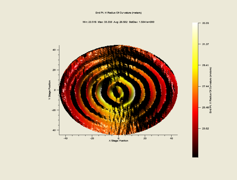
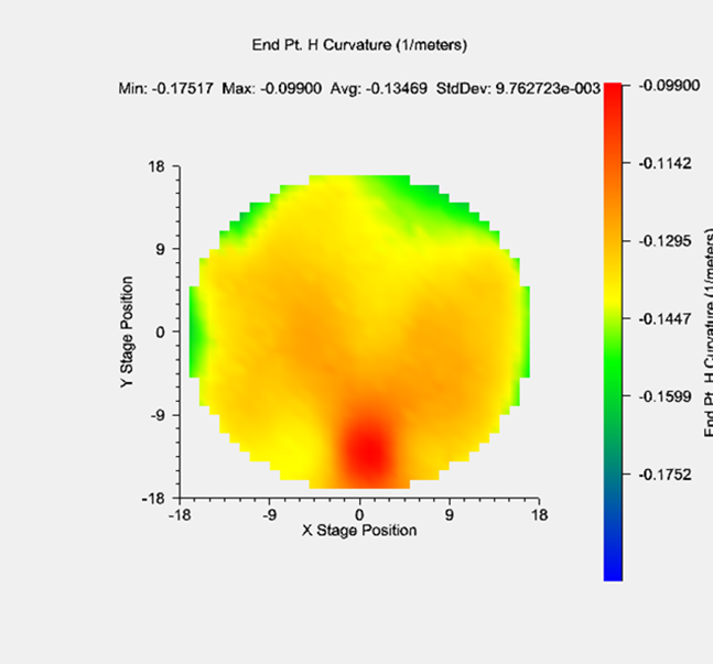
Thin-Film Curvature
kSA MOS UltraScan is equipped with both flat and curved reference mirrors for quick and easy curvature calibration. The curvature of your wafer (or other reflective surface) is measured directly from the laser spot spacing, resulting in high accuracy single point and scanning curvature measurements. Using sophisticated image processing and data analysis algorithms, the kSA MOS UltraScan can easily detect sub-micron changes in spot position due to changes in sample curvature. This makes it the highest wafer curvature and stress resolution metrology tool available.
 Click to Enlarge
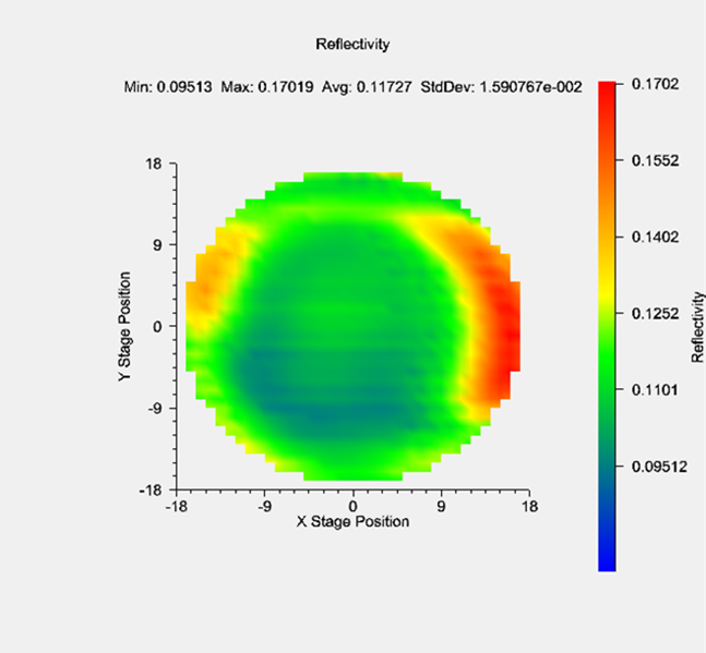
Absolute Reflectance
Absolute reflectance of the wafer (or other sample) at the laser wavelength is determined by measuring the integrated intensity of the laser spots on the camera , and is automatically calibrated before each scan by using the integrated flat mirror. This provides useful information about the quality and uniformity of the sample surface, as well as interference effects for film stacks.
Bow Height
When a laser is reflected off a bowed sample, the reflected angle will differ at different points on the wafer (or other sample). The automated laser tracking in the kSA MOS UltraScan optics not only keeps the laser array centered on the detector but also measures the changes in the angle of reflection of the laser array in order to determine the local wafer bow height and surface tilt angle.
Film Stress
To generate a thin-film stress map of a wafer, the local curvature of the wafer must be determined both pre- and post-deposition. The point-by-point thin-film stress is determined based on the change in the point-by-point curvature from the pre- and post-process curvature maps, as well as the substrate thickness, the biaxial modulus of the substrate and the film thickness. The changes in stress of a thin film after processing may also be determined from the wafer curvature maps measured after the subsequent processing steps.
 Click to Enlarge
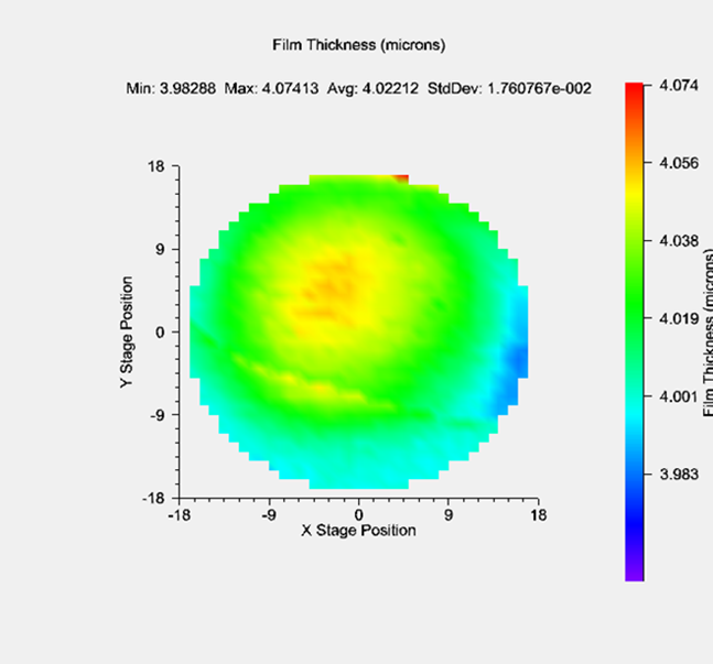
Spectral Reflectance and Film Thickness (optional add-on)
This option equips the kSA MOS UltraScan optics with a light source and a fiber coupled spectrometer. This allows the spectral reflectance of the wafer (or other sample) to be measured at each point on the sample. Using kSA’s proprietary software to measure the extrema positions in the spectral reflectance spectra, the kSA MOS UltraScan can determine the point-by point thickness of semitransparent thin films on a substrate. This data can be mapped along with other measurement parameters such as wafer curvature and film stress. Alternatively, the spectral reflectance data can be exported for multi-layer thickness or device modeling in other software programs.

kSA MOS ThermalScan includes all the capabilities of the kSA MOS UltraScan, and adds an integrated heating chamber with process gas introduction capabilities for wafer thermal stress analysis up to 1000 °C. Scans are fully programmable and extremely repeatable for selected area, line scan, or full area map of wafers (depending on model selected). The system also provides quantitative film stress analysis with full area spatial map by first scanning the bare substrate and then re-scanning the wafer post-process. Unmatched wafer curvature, stress, and bow analysis capabilities are at your fingertips for obtaining large sample uniformity profiles and/or localized isolation of sub-millimeter areas of interest with very high spatial resolution.
References
View All ReferencesEffects of Radio Frequency Bias on the Structure Parameters and Mechanical Properties of Magnetron-Sputtered Nb Films
Zegang Ni, Yuan Zhong, Xingfu Tao, Wei Li, Huifang Gao, and Yan Yao
Evident Glass Relaxation at Room Temperature Induced by Size Effect
Boyang Sun, Wenhui Cao, Zijian Wang, Baoan Sun, and Weihua Wang
Germanium thin film manufacturing using covalent bonding process
K Abadie, F Fournel, C Morales, F Mazen, L Vignoud, J-P Colonna, and J Widiez
Data-driven discovery of a universal indicator for metallic glass forming ability
Ming-Xing Li, Yi-Tao Sun, Chao Wang, Li-Wei Hu, Sungwoo Sohn, Jan Schroers, Wei-Hua Wang, & Yan-Hui Liu
Thermal Annealing on the Soft Magnetism, Microwave Properties, and Magnetostriction in Co-Fe-C Alloy Films
Jiawei Wang, Yuyi Wei, Yifan He, Cunzheng Dong, Xianqing Lin, Huaihao Chen, Xianfeng Liang, Chengju Yu, Mingmin Zhu, Yi Zhang, Jun Ni, Nian X. Sun
Plasma-assisted electron beam evaporation of low stress aluminium films for MEMS applications
Shreyas P. Bhat, Khawaja Nizammuddin Subhani, & Savitha Purakkat
