Harness the power of this patented technology to improve your process control. Measure and control uniformity, thickness, band gap, temperature, surface roughness and more.
k-Space manufactures state-of-the-art in situ, real-time thin-film deposition monitoring tools, and has
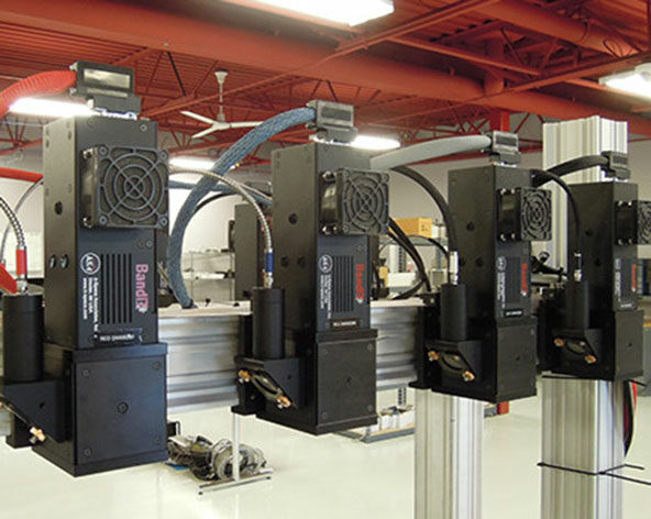
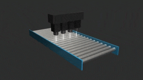
over 25 years of experience in the thin-film metrology field. The application of these proven kSA technologies to in-line PV manufacturing was a natural extension of our product line, as the most promising PV materials are based on thin-film semiconductor materials. Thin-film thickness, uniformity, band gap, and other physical properties are all critical parameters which influence PV device performance and can now be measured during the process. kSA BandiT PV technology is based on real-time spectroscopy of diffusely reflected light from a semiconductor as measured in-line during PV panel manufacturing.
A broadband light source supplies the light which is focused onto the sample. The diffusely reflected light is then collected at a non-specular angle using a lens system. The light is coupled to a high-speed, solid-state spectrometer which is then analyzed in real-time for isolating optical metrics of interest. kSA BandiT PV is applicable to materials which are deposited onto glass, metal back-coated, flexible, or directly onto semiconductor substrates. All components used are solid state, with no moving parts, to ensure highest performance and reliability.
Key Parameters
Key parameters which are measured by BandiT PV to increase performance and yield are:
 Click to Enlarge
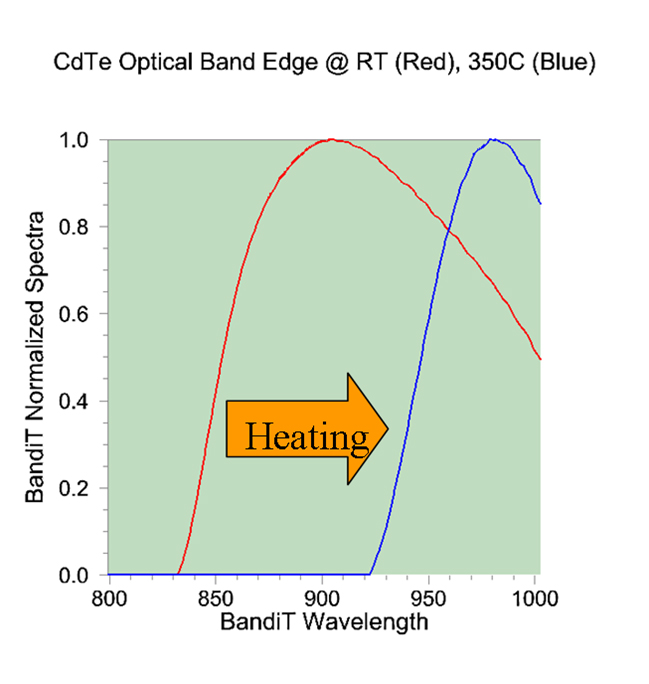
Optical Band Gap
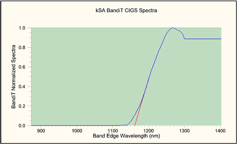
Knowledge of the wavelength of the absorption edge (Optical Band Gap) is critical to understanding the performance of photovoltaic materials. This parameter is found by analyzing the absorbed and transmitted light signature of the material to observe the material’s transition from absorbing to transparent. kSA BandiT PV and has demonstrated the capability to measure this the optical band gap for the major PV materials being manufactured today, including cadmium sulfide (CdS), cadmium telluride (CdTe), and copper indium gallium diselenide (CIGS).
 Click to Enlarge
Optical Absorption Profile
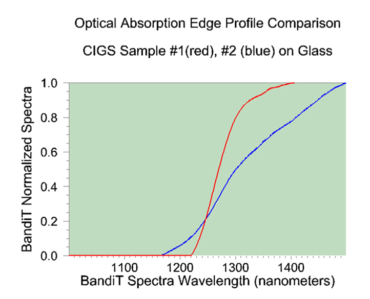
In addition to providing important optical band gap information in real-time, kSA BandiT PV can also analyze and compare the actual optical absorption shape/slope profile of the material. With this method, the absorption spectra vs. wavelength can be monitored and tuned for abruptness of the interface at the optical band gap. In this fashion, the materials properties can be modified to provide the desired optical characteristics through process tuning or heat treating.
 Click to Enlarge
Sample Temperature
The measured optical band gap of a semiconductor has a nearly linear dependence on temperature. This temperature dependence forms the basis of band-edge thermometry (BET), which has been utilized in the kSA BandiT semiconductor temperature measurement systems. kSA band-edge based technology relies upon the direct semiconductor optical absorption shift with temperature (band gap dependence on temperature). By fitting the optical absorption edge of the semiconductor in real time and using substrate-specific, kSA-generated calibration files, measurement accuracy and repeatability are guaranteed and unmatched by any other optical temperature monitoring technique.
 Click to Enlarge
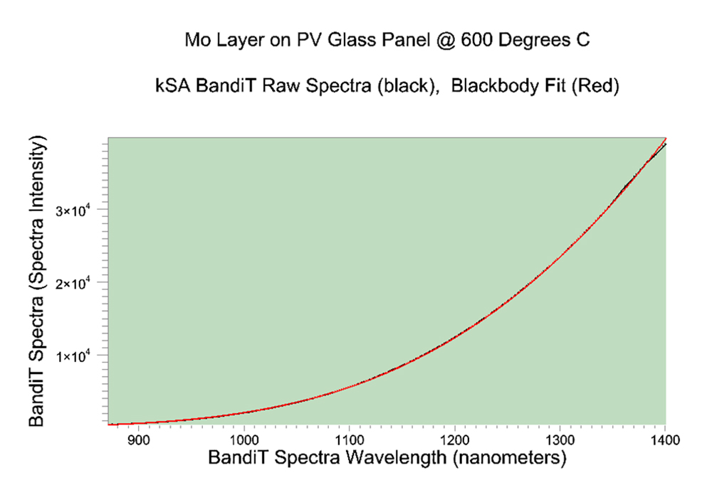
Blackbody Emission Monitoring
kSA BandiT also combines a new, patented Blackbody emission monitoring technology whereby the spectral radiation intensity of a sample is fit in real time to Planck’s equation to determine temperature. This technique is used for direct temperature measurement of the metal foil or film before the PV semiconductor layers have been deposited. Please see the kSA BandiT Blackbody technical note for additional information.
 Click to Enlarge
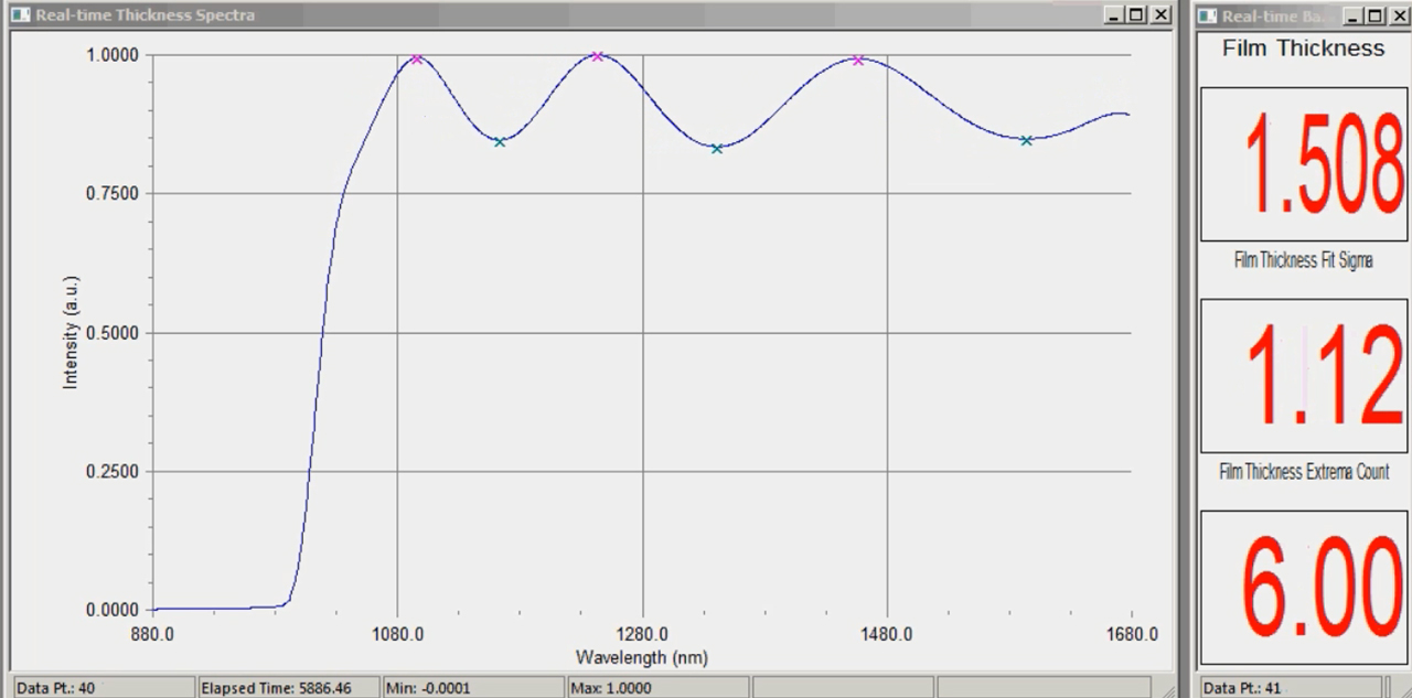
Film Thickness
Another parameter critical to the performance of photovoltaic devices is the active layer or TCO thickness. kSA BandiT PV uses spectral reflectivity to real time, in situ measurements is based on analyzing the interference fringes observed in the reflectance spectrum from a film. Spectral reflectance spectra from thin films exhibit interference patterns due to light interference based on the film’s thickness. Using the known film’s refractive index dispersion, the film thickness can be determined by analyzing the extrema positions of the interference fringes. With advanced kSA BandiT PV software models, film thickness changes of 1nm can be measured.
 Click to Enlarge
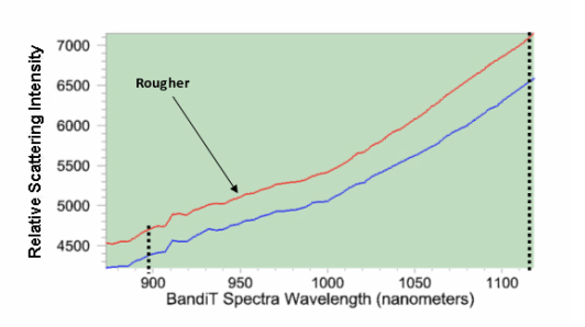
Surface Roughness
Surface roughness is one of the critical parameters affecting solar module efficiency. These surfaces are often intentionally roughened during the deposition process, as an optimally textured surface will absorb more solar radiation than a perfectly smooth one. kSA BandiT PV can get a relative measure of roughness by looking at the “above-gap” scatter from the surface. In theory, any light that has a wavelength sufficiently above the band gap energy should be completely absorbed by the semiconductor layer(s). The amount of scatter is a direct indication of the relative roughness of the surface. We therefore can sum the “above-gap” intensity to determine a relative roughness metric. This metric may also be calibrated directly against a sample of known surface roughness, providing a real-time, in situ quantitative roughness parameter.
