
 Researchers at k-Space Associates, Inc. were awarded a U.S. patent (number US 9,030,652 B2) for reflectivity triggering technology for free rotating wafer carriers.
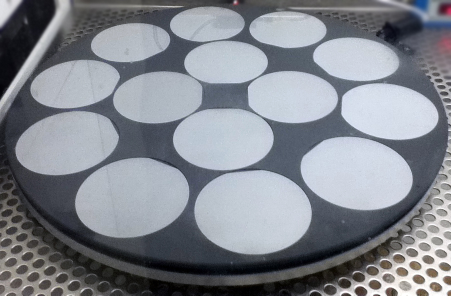
With this technology, reflected light from a rotating wafer carrier is detected and processed by a microcontroller. The microcontroller is programmed to analyze the reflected signal in real-time in order to generate a trigger signal that is synchronized to the rotating carrier. This signal can then be used to trigger data acquisition at user defined markers, for example, on the center of all wafers or even multiple positions on each wafer. The algorithm and microcontroller are fast enough to synchronize to carriers rotating at up to 1,800 rpm. This ensures that measurements are taken at precise positions across the carrier, providing accurate process control data. Ultimately, this technology leads to both faster device development and superior device quality and performance.
This new capability is incorporated into k-Space metrology tools designed to measure in situ, real-time thin-film growth parameters, like growth rate, temperature, and wafer curvature. It is advantageous in multi-wafer systems where there is not a positive mechanical lock between the motor driven spindle and carrier. Without the lock, the angle of the platen may drift over time, making the standard “home pulse” signal invalid for wafer/carrier synchronization.
k-Space’s CEO, Darryl Barlett, commented, “Without this ‘soft trigger’ capability, many of our in situ metrology tools would not be able to take wafer-specific measurements, which significantly reduces the usefulness of the metrology tool.”
This technology was invented by k-Space employees Scott Hines, Darryl Barlett, Chuck Taylor and Greg DeMaggio. This is the fifth U.S. patent awarded to k-Space Associates, Inc. involving thin-film measurement.
About k-Space Associates, Inc.
k-Space Associates, Inc. (www.k-space.com/) is a leading supplier of advanced instrumentation and software for the surface science and thin-film technology industries. Founded in 1992, its systems are used for monitoring wafer temperature, thin-film stress, deposition rate, thickness, material absorption properties, and Reflection High Energy Electron Diffraction (RHEED). Backed by a commitment to ongoing support, these solutions are currently used worldwide in research and production line monitoring of compound semiconductor-based electronic, optoelectronic, and photovoltaic devices. Extensive input and close collaboration with its worldwide customer base has led to the development of today’s most powerful thin film characterization products
