
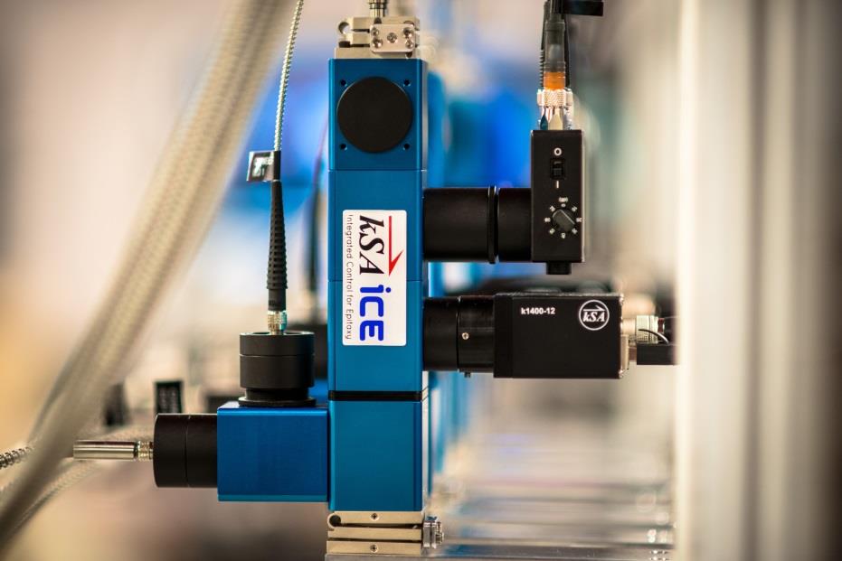
 k-Space Associates, Inc. (www.k-space.com/) is proud to announce that NuFlare Technology, Inc. (Kanagawa, Japan, www.nuflare.co.jp), a leading manufacturer of semiconductor equipment, has installed multiple kSA ICE (Integrated Control for Epitaxy) in situ metrology tools for process monitoring and control. These kSA ICE tools measure real-time wafer temperature, curvature, and reflectance for NuFlare’s custom, multi-chamber MOCVD reactors focused on the growth of GaN on 200mm Si substrates.
The NuFlare MOCVD system can be configured with up to four, single-wafer, 200mm MOCVD process modules. k-Space worked with NuFlare to develop a custom kSA ICE tool that allows for simultaneous real-time measurement from multiple measurement heads on each process module from a single controller. This helped to reduce the total system costs while maintaining full monitoring and control capabilities.
These ICE tools perform patented curvature measurements that are critical to successful GaN on Si integration. Moreover, by measuring the temperature of the wafer via emissivity-corrected pyrometry (ECP) at two positions on the wafer, users obtain temperature control to better than 1°C. This kSA ICE multi-chamber design allows measurement heads to be easily added as a customer moves from one process module up to four 200mm process modules.
Dr. Chuck Taylor, head of product development at k-Space, commented, “NuFlare worked side-by-side with us to help develop a kSA metrology tool tailored to the needs of this growing market. We believe that the modular capability of this custom kSA ICE tool is an ideal cost effective solution for a multi-module MOCVD system.”
To discover more about in-situ metrology tools for thin-film characterization visit www.k-space.com/.
About k-Space Associates, Inc.
k-Space Associates, Inc. (www.k-space.com/) is a leading metrology supplier of advanced instrumentation and software for the surface science and thin-film technology industries. Founded in 1992, its systems are used for monitoring wafer temperature, thin-film stress, deposition rate, thickness, material absorption properties, and Reflection High Energy Electron Diffraction (RHEED). Backed by a commitment to ongoing support, these solutions are currently used worldwide in research and production line monitoring of compound semiconductor-based electronic, optoelectronic, and photovoltaic devices. Extensive input and close collaboration with its worldwide customer base has led to the development of today’s most powerful thin film characterization products.
