
k-Space Associates, Inc. (www.k-space.com/) is pleased to announce the release of the kSA Scanning Pyro, an in-situ tool designed to measure temperature variations across Veeco K465i wafer carriers. MOCVD fabs generally perform spot temperature measurements on wafer carriers to help tune the heater zones in an attempt to achieve uniform temperature profiles. Making use of the K465i’s slit viewport, the kSA Scanning Pyro utilizes a custom dual pyrometer to acquire a complete, high resolution carrier temperature map in a single scan. The tool can easily be adapted to other MOCVD tools, including the Aixtron G4 and G5, and the Veeco EPIK700.
“This tool is designed to quickly, easily, and accurately generate full carrier temperature maps on Veeco K465i and EPIK700 production MOCVD reactors. The kSA Scanning Pyro generates high-resolution, full carrier temperature maps to facilitate near real-time temperature adjustments and to identify hot/cold spots on carriers and wafers. MOCVD fabs with this tool can expect to have a competitive advantage in terms of yield, wafer uniformity and device performance,” commented Darryl Barlett, CEO of k-Space Associates, Inc.
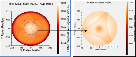
The kSA scanning Pyro uses technology that combines simultaneous temperature measurements from two scanning sensor heads to map the entire carrier, from center thru the outer edge. Users can acquire either a full wafer carrier scan or a select sub-set of the full scan, and can then perform analysis with proprietary kSA software to identify problem areas. With this information in hand, engineers can make the necessary process and/or hardware adjustments to improve their product.
This is the second new product that k-Space Associates has introduced in 2015. The first, kSA SpectraTemp for absolute temperature measurement, is used for absolute temperature calibration and measurement, or to calibrate the kSA Scanning Pyro tool. To learn more about either tool visit www.k-space.com/.
About k-Space Associates, Inc.
k-Space Associates, Inc. (www.k-space.com/) is a leading supplier of advanced instrumentation and software for the surface science and thin-film technology industries. Founded in 1992, its systems are used for monitoring wafer temperature, thin-film stress, deposition rate, thickness, material absorption properties, and Reflection High Energy Electron Diffraction (RHEED). Backed by a commitment to ongoing support, these solutions are currently used worldwide in research and production line monitoring of compound semiconductor-based electronic, optoelectronic, and photovoltaic devices. Extensive input and close collaboration with its worldwide customer base has led to the development of today’s most powerful thin film characterization products.
