
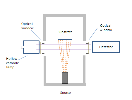
Dexter, MI, March 5, 2015 – k-Space Associates, Inc. has received a Small Business Innovation Research (SBIR) Phase 1 grant from the DOE (Department of Energy) Office of Science to develop an atomic absorption spectroscopy (AAS) tool. Once fully developed, the AAS tool will perform in situ measurements of the flux density of individual species such as silicon, aluminum and metal-silicides. This will allow for precise control of deposition rate over long time periods to produce high-quality films.
The goal of the SBIR Phase I work will be the development of a multi-species, AAS-based film growth monitor that is robust and non-intrusive, with very low long-term drift, high material selectivity and sensitivity, fast response time, and wide operating pressure range capable of covering both ultra-high vacuum (UHV) and sputtering processes. With its high sensitivity and long-term accuracy under continuous operation, it should find immediate application in the fabrication of multilayer Laue lenses (MLLs), as well as many other thin-film products including lasers, photovoltaics, and LEDs, to name a few.
k-Space Associates’ CEO Darryl Barlett says, “We investigated several different potential technologies for this flux monitor, including tunable lasers and broadband white light sources. In the end, the Hollow Cathode Lamp (HCL) approach offers the most flexibility and cost effectiveness. Combining the HCL sources with new solid-state spectrometer technology, we’re confident that we can develop a very stable and high sensitivity flux monitor under this Phase I effort.”
It is expected that the proposed instrument, when successfully developed, will become a standard tool for both the R&D and manufacturing of thin-film devices.
About k-Space, Associates, Inc.
k-Space Associates, Inc. (www.k-space.com/) is a leading supplier of advanced instrumentation and software for the surface science and thin-film technology industries. Founded in 1992, its systems are used for monitoring wafer temperature, thin-film stress, deposition rate, thickness, material absorption properties, and Reflection High Energy Electron Diffraction (RHEED). Backed by a commitment to ongoing support, these solutions are currently used worldwide in research and production line monitoring of compound semiconductor-based electronic, optoelectronic, and photovoltaic devices. Extensive input and close collaboration with its worldwide customer base has led to the development of today’s most powerful thin-film characterization products
