
Dexter, MI. April 30, 2105 – k-Space Associates, Inc. (www.k-space.com/) announces a new auto exposure capability available for the kSA 400 analytical RHEED system. The auto exposure control feature automatically adjusts the exposure time of the kSA 400 camera as the RHEED pattern intensity increases or decreases so that signal saturation or low signal levels do not occur and important data isn’t lost. The intensity measured in user-specified regions is automatically scaled with the exposure time so that both the real-time plots and recorded data reflect the correct intensity over the course of the acquisition. This feature is included with all new kSA 400 software upgrades and kSA 400 system purchases.
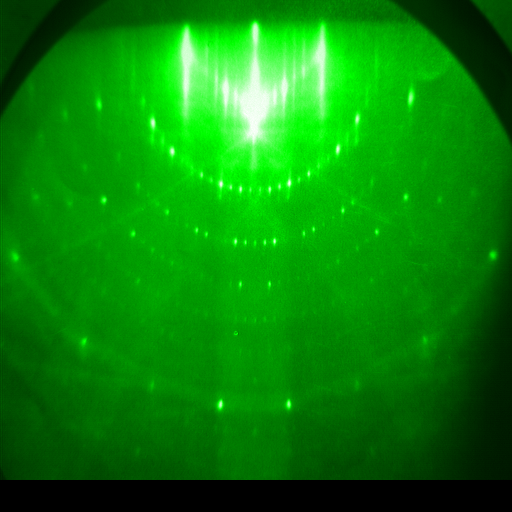 k-Space CEO Darryl Barlett comments “RHEED patterns inherently have a very large dynamic range. In addition, the pattern can change significantly during deposition, due to interference, roughening, desorption, etc. By utilizing the large exposure time range of the kSA 400 cameras, we can compensate in real-time for the changing RHEED pattern, assuring that adequate data is collected throughout an entire deposition run or surface study. It’s similar to using an auto gain control capability on video cameras, except in this case the integrity of the absolute intensity values is maintained.”
kSA 400 analytical RHEED systems are used worldwide in MBE, PLD, Sputtering and other thin-film deposition chambers providing important feedback for growth rate, surface roughness, lattice spacing and structural analysis.
Click here to see a video demonstrating auto exposure control.
About k-Space Associates, Inc.
k-Space Associates, Inc. (www.k-space.com/) is a leading supplier of advanced instrumentation and software for the surface science and thin-film technology industries. Founded in 1992, its systems are used for monitoring wafer temperature, thin-film stress, deposition rate, thickness, material absorption properties, and Reflection High Energy Electron Diffraction (RHEED). Backed by a commitment to ongoing support, these solutions are currently used worldwide in research and production line monitoring of compound semiconductor-based electronic, optoelectronic, and photovoltaic devices. Extensive input and close collaboration with its worldwide customer base has led to the development of today’s most powerful thin film characterization products.
