Applications
kSA thin-film metrology instruments are used in a wide range of deposition processes. kSA products measure and provide thin-film process control for important parameters such as temperature, deposition rate, film thickness, stress, curvature, bow, reflectivity, surface roughness, and many other material properties. These are measured in real-time by utilizing probes such as lasers, white light, UV light sources, and electron beams to investigate at an atomic level.
Our thin-film analysis tools are used to extract real-time information from today’s most advanced deposition and processing applications within compound semiconductor, silicon semiconductor and photovoltaic advanced thin film production and R&D.
Sophisticated software analysis and reporting capabilities provide information to better understand the end product or to provide online control during mass production to enhance yield. Tailored optics and fully integrated solutions have been designed for simple mounting and non-invasive monitoring of many applications such as:
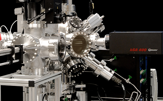
Molecular Beam Epitaxy (MBE)
Obtain unmatched process efficiency and quality with powerful tools for...
Metalorganic Chemical Vapor Deposition (MOCVD)
Increase performance and quality with compact in situ tools for...
Sputtering
Monitor and control your sputtering deposition process with in situ...
Thermal and E‑beam Evaporation
Advanced optical device fabrication calls for advanced technologies like in...
Physical Vapor Deposition (PVD)
Increase quality with controlled deposition, stress monitoring and RHEED analysis...
Pulsed Laser Deposition (PLD)
Analyze and control your Pulsed Laser Deposition (PLD) while deposition...
