Leaders in thin film and industrial metrology
Putting Light to WorkSince 1992
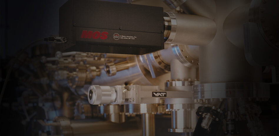
Thin Film Metrology
Leading manufacturer of in-line, in situ, and ex situ metrology tools for the semiconductor and thin-film industries.
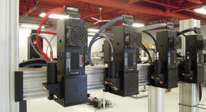
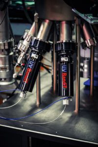
Industrial Metrology
Custom non-contact measurements and software integration for production environments. Measure and control uniformity, dimensions, surface characteristics, and more with our many industrial metrology tools.
World Class Technical Support
We take pride in providing the best technical support in the industry. No automated queues, no slow response times. When you call, you’ll always get a friendly k-Space person to direct your call to the appropriate engineer. Or, contact us via email – we guarantee we’ll respond within 1 business day. Contact us today so we can discuss your metrology needs.
We also provide our customers full access to the k-Space Knowledge Base. The k-Space Knowledge Base is filled with troubleshooting advice, a helpful video library, tricks of the trade, and much more. Email us for login information.
We look forward to hearing from you!
About k-Space
Incorporated in 1992 and driven to supply the best technical support in the industry, our tools are used worldwide in both research and full production monitoring and process control for glass, automotive, building materials, semiconductor, PV, thin-film deposition, annealing, processing, and more.
